Lab 3 - Building an ALU
For this lab you will implement the major pieces of a 1-bit ALU. If you are confident in your breadboarding skills, you can try to fit all of the components on your board at once and connect them together at the end to build a complete ALU, but this is not required.
A warning about damaged TTL chips: I have found several damaged TTL chips during my preparations for this lab. I recommend quickly testing each chip logic switches and your logic probe to verify that the gate works correctly. Inverters have a tendency to fail and become “always on gates,” which can be difficult to find once your circuit is built!
1. Build a one bit full adder
Using the logic diagram below, build a full adder.
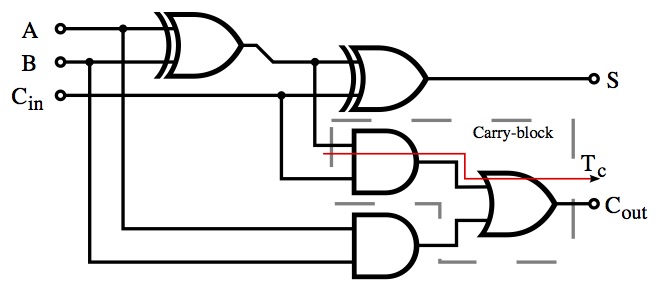
Write a truth table for the full adder and test it to verify that your circuit is working correctly.
2. Build a two bit decoder
Use four AND gates and two NOT gates to build a two bit decoder. One way to think of a decoder is a binary to unary converter: the two input bits specify a binary number. That number determines which output line is turned on, while the rest are off.
Don’t disassemble your decoder if you are planning to build the full ALU on your board; you will use it in the next step to build a four input multiplexer.
3. Finish your ALU (optional)
You can turn a two bit decoder into a four input multiplexer with four AND gates and three OR gates. Use the two inputs to your decoder as the selector lines. Use four logic switches as your multiplexer input (for now). Connect each input to an AND gate, along with one of the decoder outputs. Connect all the AND gate outputs to a four-input OR gate, which you will have to construct from two-input OR gates. The logisim circuit below shows this circuit, using your existing decoder:
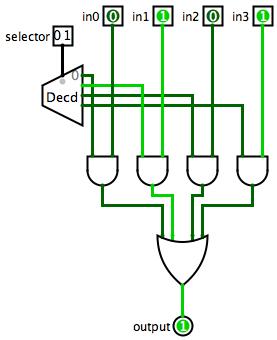
If you saved your adder circuit, connect it to your multiplexer input. Add AND and OR operations to your ALU if you have time.
Acknowledgements
This lab is adapted from Janet Davis’ lab in 2013. The circuit diagram for the full adder is from Wikipedia, and has been placed in the public domain.
#/media/File:Full-adder_logic_diagram.svg)