Lab 2: Problem Solving with Logic Gates
Summary: In this lab you will use logic gates in a circuit to solve a logical puzzle. Instead of building logic gates using transistors, we will use TTL chips, which have several logic gates in a single chip.
Due: Monday, September 12 by 5pm
Submitting your work: Please show your completed work to me or the mentors during lab time, or arrange an alternate time to demonstrate your solution during office hours.
Groups
- Adam W., Sophie, and Maddie
- Linda and Giang
- Fengyuan and Eli
- Devin and Theo
- Ryan and Ana
- Bea and Hattie
- Matt and Jacob
- Sara and Charlie
- Blake and Hamza
- Adam H. and Tanner
- Kamal and Jerry
The Problem
There is an old puzzle in which a farmer F must transport a wolf W, a
goat G, and a cabbage C across a river. However, the farmer can only
transport one of W, G, or C across the river at a time, and if left
together and unattended, the goat will eat the cabbage and the wolf will eat
the goat. Let F=0 indicate the presence of the farmer on the west bank of
the river and F=1 indicate presence on the east bank. Use similar
definitions for W, G, and C.
Lab Work
I expect that you will be able to complete this work during normal lab time. Please show your work to me or a mentor after each step in the lab work section below. If you are unabel to finish all of the steps below during our scheduled lab, you may save your circuit on the board. Once you have completed the lab, schedule a time during my office hours where at least one member of your group can demonstrate your completed lab and show
- Derive a truth table defining a function which gives 1 if the farmer is in danger of losing the goat or the cabbage. You may assume that a trip across the river can be made instantaneously, so that if an item (or farmer) is not on one side of the river it must be on the other side.
- Use a Karnaugh map to generate a sum-of-products expression for this function. Then simplify the expression further with boolean algebra. Your final result should include only 8 variables, including repeated occurrences of the same variable.
- Draw a logic circuit diagram that implements your function from step 2. Label parts of the circuit that should be wired to the logic indicators on your protoboard to show when the farmer is in danger of losing either the goat or the cabbage.
- Using TTL chips, construct and test a circuit that implements your circuit diagram from step 3.
- Propose a solution to this puzzle starting with
F,W,G, andCinitially on the west bank and must be transported to the east bank. Use your circuit to check your solution.
Hints
- Check the part number on each chip carefully as you get it from the supply cabinet, and as you put it back. If you can not see the number well, hold it up to the sunlight. This is can be surprisingly helpful.
- Make a diagram of your physical circuit as you build it, recording where each gate in your logic circuit diagram is located on the protoboard.
- As you make each physical connection between logic gates, check the connection off in your logic circuit diagram.
- Either arrange your switches for
F,W,G, andCin the same order as they are in your truth table, or be very careful to translate between the two correctly when testing your circuit.
Background
TTL chips look approximately like this. They are 14-pin “dual in-line packages” (DIPs), meaning that the chips are long and narrow with 7 pins on each side. Each chip has a small notch in one end for orientation. When the notch is pointed upward as in the diagram, the pins are numbered from 1 to 14 starting in the upper-left corner and proceeding counter-clockwise.
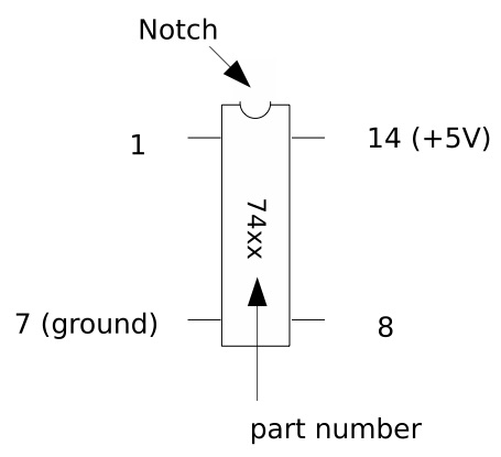
For purposes of your logic design, note we have the following TTL chips available in the lab:
- 1-input inverter (NOT) (6 gates per chip);
- 2-input AND, OR, NAND, NOR, XOR (4 gates per chip);
- 3-input AND (3 gates per chip).
I will provide a pinout diagram, showing what each pin on each chip is for. Please note that the pinout for different chip types (AND, OR, etc) is different.
Please note carefully, that you must connect each chip to power and to ground. It is important that you use the correct pins for this. Reversing power and ground will damage the chip. Make sure you connect to +5v and ground, not the adjustable +v or -v rows.
Seating chips in the board
Please refer to the protoboard diagram provided in the lab handout, to locate the “channel” between banks of pin connection points. To seat a chip in the protoboard, orient it such that its notch is facing upward as in the diagram, then place its two rows of pins such that they straddle one of the valleys in the board. This helps you attach power and ground to the correct pins, and ensures that none of the pins are connected together.
The chips may take some careful coaxing to seat them properly. I suggest placing one row of pins loosely into their holes in the board, and then using a fingernail to get the other row of pins lined up and started into their holes. Once all pins have been started correctly, you can press firmly, and the chip should snap into place. (Please be gentle until the pins are started well, or they will get bent, but then do press firmly to make sure the chip is fully inserted and that each pin makes a good connection with the board.)
Removing chips from the board
Be careful not to pull chips out of the board at an angle, which could bend or break the pins. Grab the chip at the top and bottom edges (where the chip crosses the channel on the protoboard). If you cannot remove the chip by hand, we can remove it carefully using a small screwdriver.
Working with Resistors
Now that we’re working with TTL chips and the logic switches in the lower left corner of your protoboard, you can safely omit resistors from your circuits. Instead of turning the cirucit on and off, logic switches make a connection from your wire to either +5v or ground. That eliminates the need for pull-down or pull-up resistors. The other use case for resistors in our previous lab was to limit the current through transistors and LEDs. As long as you use the logic indicators on the right side of the board instead of raw LEDs, you can omit these resistors as well.
Please double-check to make sure your logic indicator and logic switch sections are set to TTL mode. While you’re double-checking your board configuration, make sure your TTL chips are powered from +5v and ground, not the adjustable +v or -v rows.
Acknowledgements
Based on the fox, goose, and bag of beans puzzle.