Lab: Build an ALU
- Assigned
- Wednesday, Sep 19, 2018
- Due
- Tuesday, Sep 25, 2018 by 10:30pm
- Summary
- For this lab you will implement the major pieces of a 1-bit ALU. This requires that you build both an adder and multiplexor on your protoboard and connect them together so be careful with your layout.
- Submitting
- After completing each exercise, show your completed circuit to the instructor or a course mentor. If you are unable to complete the lab during class time, schedule a time during office hours to demonstrate each of your circuits.
Reminders
You will once again use the TTL chips to build circuits. Please remember to:
- Orient the chips notch up
- Connect Vcc to +5v and ground the chips
- Wire them carefully to avoid destroying them
You can find a TTL pinout diagram printed in the cabinet or in this pdf.
Remember also that it can help to label the coordinates of your physical wires on your circuit diagrams.
Part 1: Build a one-bit full adder
Using the logic diagram below, build a full adder on your protoboard.
Plan carefully; you will need to leave space to build a multiplexor from a decoder on your board in the next two parts of the lab.
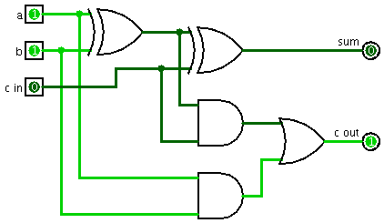
Test your circuit using the truth table in Figure B.5.3 (p. B-27) of your textbook.
Part 2: Build a two-bit decoder
One way to think of a decoder is a binary to unary converter: the two input bits specify a binary number. That number determines which output line is turned on, while the rest are off.
- Draw a circuit diagram for a two-bit decoder using four AND gates and two NOT gates.
- Build your two-bit decoder on the protoboard using the TTL chips.
Don’t disassemble your decoder—you will use it in the next step to build a four-input multiplexer.
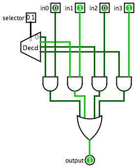
Part 3: Build a four-input multiplexor
Turn your two-bit decoder into a four-input multiplexer by adding four two-input AND gates and three two-input OR gates, as follows.
Use the two inputs to your decoder as the selector lines. Use four logic switches as your multiplexer input (for now). Connect each input to an AND gate, along with one of the decoder outputs. Connect all the AND gate outputs to a four-input OR gate, which you will have to construct from two-input OR gates. The logisim circuit below shows this circuit, using your existing decoder:
Part 4: Finish your ALU
Now that you have a one-bit adder and a four-input multiplexor, complete your ALU with AND and OR gates. Use the selector in your multiplexor to choose between addition (selector at 00), logical AND (selector at 01), and logical OR (selector at 10).
Extra Challenge: Subtraction
If you still have time, add a binvert input so that your ALU can subtract as well as add.
- Using
bandbinvertas inputs, draw the truth table for a one-bit selector whose inputs are $b$ and $\overline{b}$ with thebinvertcontrol signal. (You should find the resulting circuit to be simpler than a general one-bit selector with two independent inputs.) - Wire the appropriate gate(s) to conduct the one-bit subtraction.
- Set the
binvertandcarry_ininputs and test that your ALU implements subtraction correctly.
Copyright © Marge Coahran, Charlie Curtsinger, Janet Davis, and Jerod Weinman
 This work is licensed under a Creative Commons Attribution-NonCommercial-ShareAlike 4.0 International License.
This website was built using Jekyll, Twitter Bootstrap, and the Bootswatch Cosmo Theme.